Emission Filters for Fluorescence Detection: Single-point versus Imaging

Introduction
IDEX Health & Science | Semrock has focused on fluorescence filters from the very beginning. Our ultra-steep spectral edge transitions, deep blocking, and high transmission specifications have set the standards for excellence and have enabled a generation of high-performance instruments for bioscience and medicine.
The emission filter is a critical part of any fluorescence system (learn more about fluorescence filters here). Emission filters, and to a lesser extent excitation filters, provide most of the signal-to-noise ratio (SNR) enhancement in fluorescence systems. This note describes emission filters and their use in both single-point (as in photometry and point-scanning) and imaging (microscopic and macroscopic) applications. For a detailed discussion of wavefront aspects, see [1].
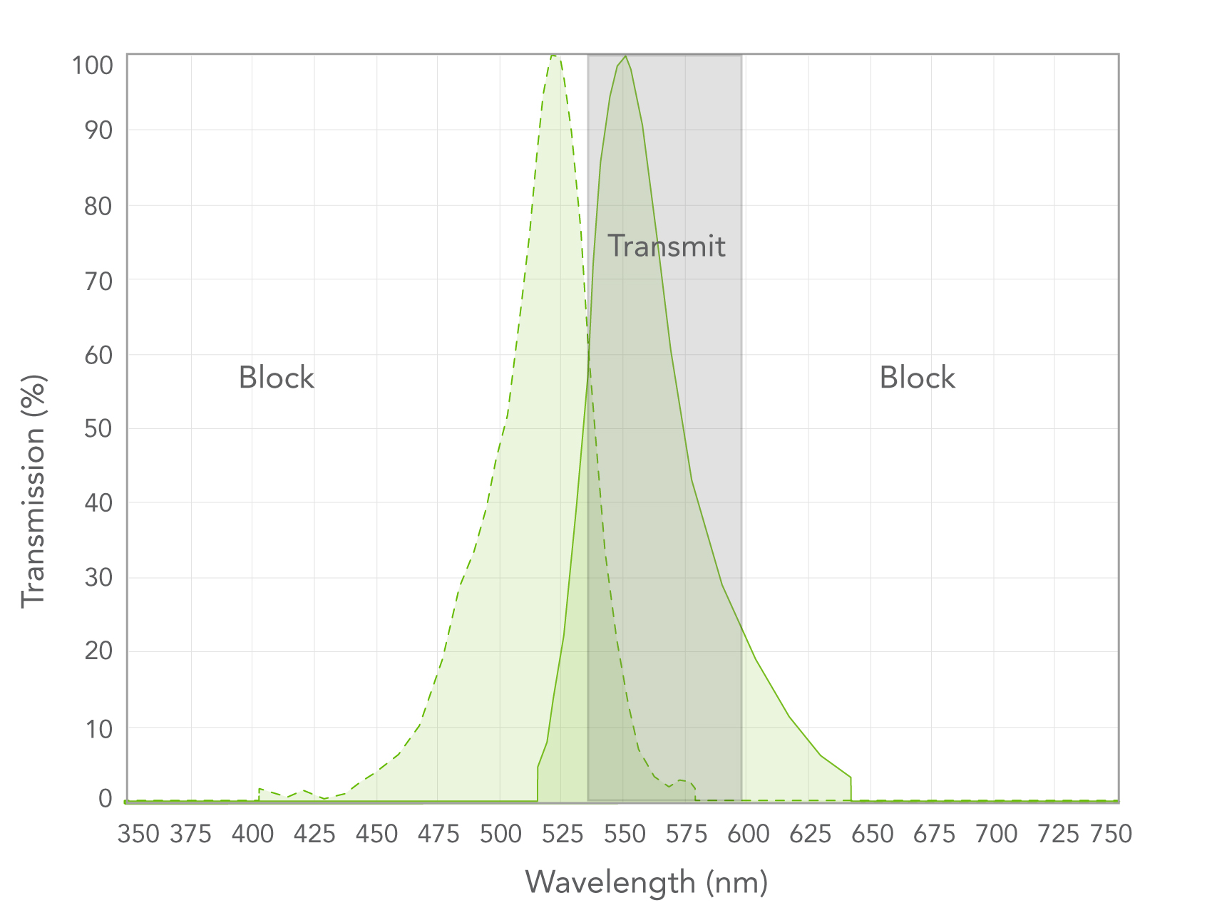
Figure 1: The transmission region should include the peak emission band while blocking the excitation band.
Fluorescence detection requires effective blocking of excitation and stray light to maximize SNR. The fluorescence emission peak should fall within or near the transmission range of the emission filter (Figure 1). The blocking level should be high (OD > 5) over the excitation region and extend through the optical sensor response range, though the blocking can be reduced at long wavelengths where the sensor spectral efficiency is low.
Optical sensors have different properties including response time, amplification, dynamic range, spectral response, and dark noise level. However, the spectral efficiency of a sensor largely depends on the materials from which it is made. Semiconductor-based sensors are often composed of doped Silicon for visible-range detection and Indium Gallium Arsenide (InGaAs) for NIR detection. These materials are used in single point sensors including photodiodes, APDs, SPADs, SiPMs as well as in area sensors such as CCD and SCMOS cameras. An older type of detector is still widely used -- the photomultiplier tube (PMT), based on a vacuum tube structure. Typical spectral response curves of the primary sensor materials are shown in Figure 2.
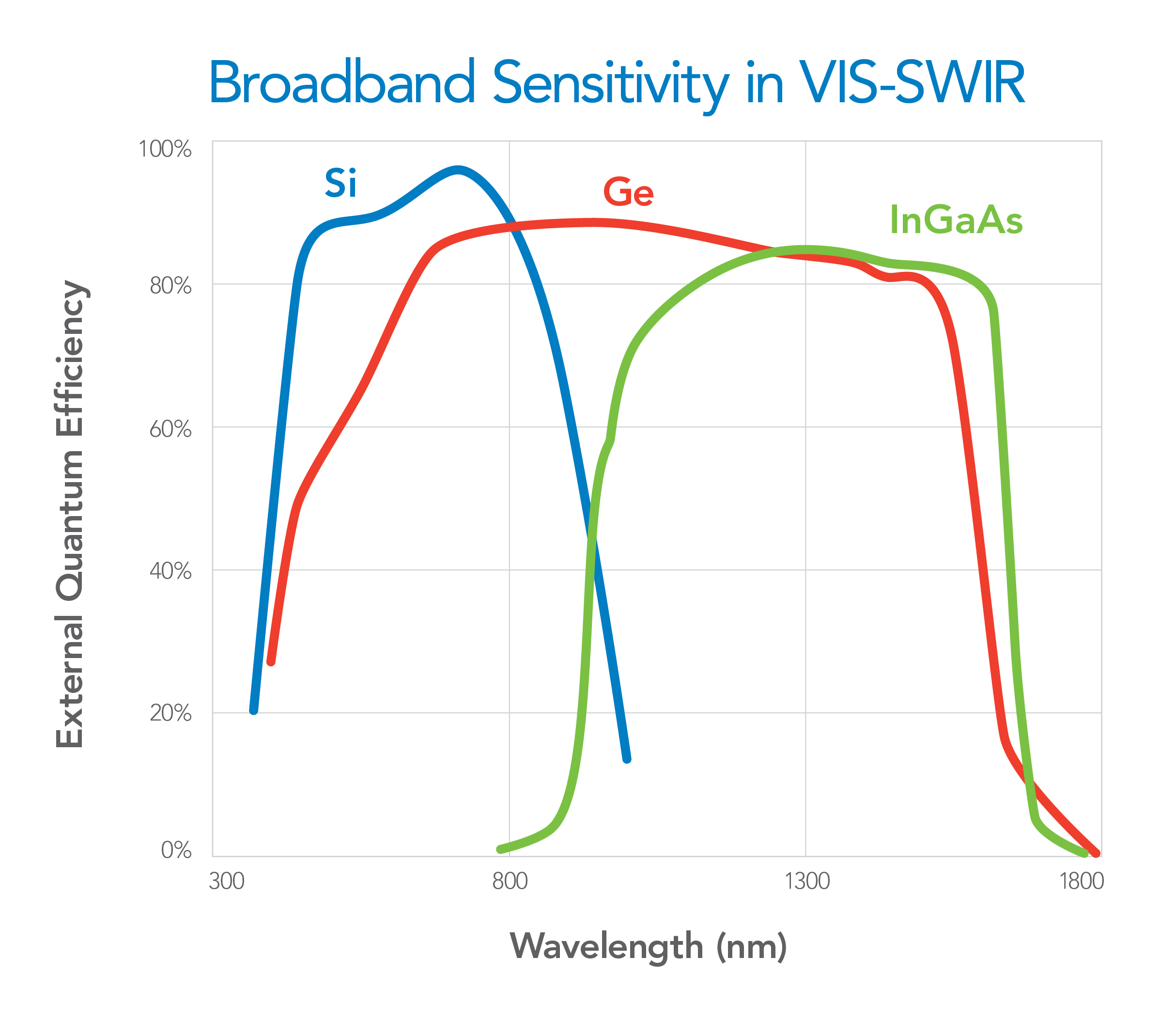
Figure 2: Typical spectral response curves of Si, Ge, InGaAs. Image data from Reference 2.
Emission Filters for Single-point Measurements
A single-point fluorescence detector measures the total integrated signal independent of the spatial light distribution. The most important filter specifications to consider are the levels and ranges of the transmission and blocking regions. If only a single fluorophore is to be used, a long-wave-pass filter rather than a bandpass filter can be used to maximize signal. However this usually increases noise (background signal) even more, so is not an optimal choice. Many systems use several emission wavelength bands detected either simultaneously (multiplexed) or serially, with dichroic beamsplitters used to move the light towards the correct bandpass filters. In these cases, crosstalk can become an issue between spectrally adjacent and overlapping fluorescent channels (Figure 3). The excitation and emission filters work together with the illumination and detection strategy to provide adequate blocking in these systems. Unless a pulsed illumination strategy is employed, emission filters’ transmission regions are narrow enough to be positioned between excitation bandpass regions and with deep blocking on both sides of the emission spectrum to minimize crosstalk from both directions.
Learn more about choosing filters for fluorescence multiplexing here
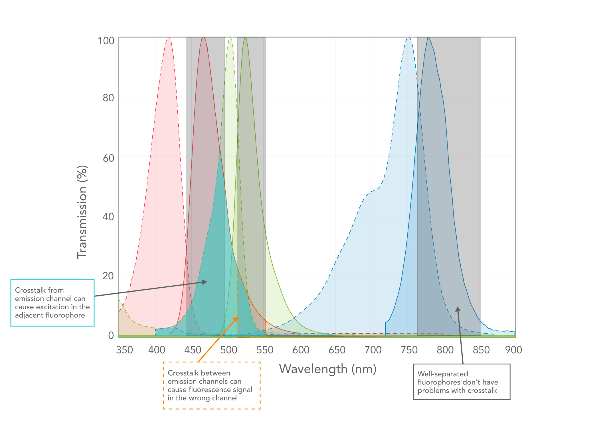
Figure 3: Image showing crosstalk between emission channels.
High OD blocking in the emission filter is required to minimize excitation light from one or multiple bands leaking into the detection channel(s). In addition, the blocking region should extend across the entire spectral response curve of the detector. The blocking should be maximal (i.e., OD > 6 or even > 8) where the excitation light is the brightest, i.e., at the peak laser or LED emission wavelength(s) and in the excitation filter’s transmission band. At the crossover point (the wavelength at which the spectral responses of the excitation and emission filters intersect) each filter should exhibit blocking of least OD 3.5 and have very high edge steepness. OD values in excitation and emission filters are usually additive, so an excitation filter with OD 3.5 and an emission filter with OD 3.5 at the same wavelength yield an effective blocking of OD 7. As described above, the emission filter’s blocking range should also cover the detector response curve. For instance, in Figure 4, the detector response curve extends out to 750 nm.
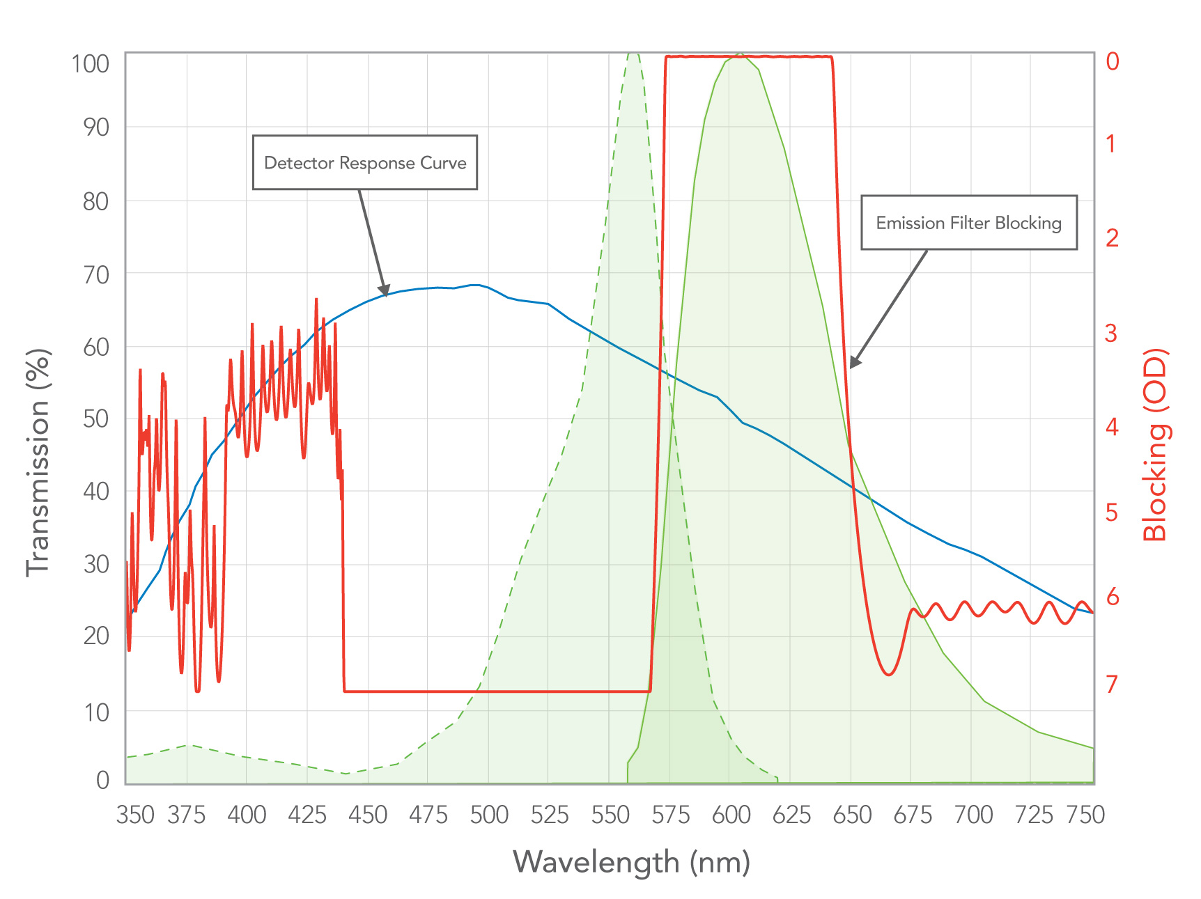
Figure 4: Overlaid spectral responses of detector, fluorophore excitation and emission, and emission filter (in OD).
Interference filters produced by a sputtering process can contain significant surface stress in the deposited films resulting in spherical aberration and wavefront errors. If a sputtered emission filter is used in the typical transmissive configuration, transmitted wavefront errors (TWE) of up to several waves per inch do not affect the integrated signal being measured if the entire beam is captured by the detector (Figure 5), as for a single-point measurement the spatial distribution of the signal is not important. Although less common, reflection by the emission filter can be used as part of the detection path, essentially using the emission filter as a dichroic beamsplitter. In this case, spherical aberrations can cause significant reflected wavefront error (RWE) that affects the focus of a reflected beam. This can result in over-filling of the detector in downstream measurements. Specifying RWE is crucial in these geometries (Figure 5), unless the aberrations can be corrected in the optical design by refocusing or calibrating the system (Click here to learn more about wavefront errors).
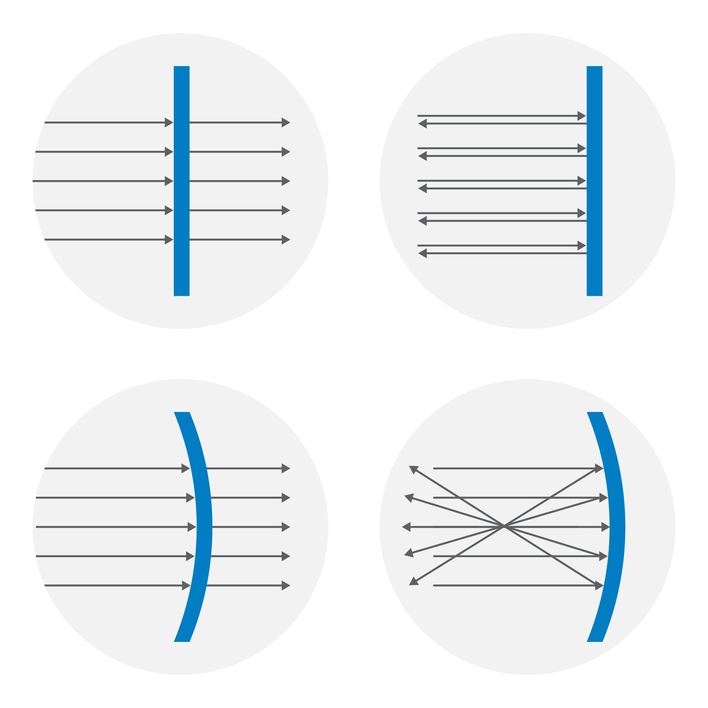
Figure 5: Spherical aberration.
Top: with no TWE or RWE, transmitted and reflected beams are unchanged.
Bottom left: when an optic with spherical aberration is placed in the transmitted beam, a slight increase in transmitted beam width is observed with a small TWE.
Bottom right: the same curved optic causes beam focusing upon reflection, resulting in a higher RWE error.
Emission Filters for Spectroscopy and Imaging
Spectroscopy using array detectors and imaging with cameras requires careful and reproducible positioning of the fluorescence signal on the detector. Wavefront errors and substrate wedge should be considered and specified for these types of applications.
Spectroscopy (fluorescence and Raman) is often performed using a linear array of detectors to reduce or eliminate the number of moving parts in the system. The light is dispersed in a single direction using a prism or grating to illuminate each element of the array detector with a different wavelength range. Flow cytometers and fluorescence microscopes with spectral detection often use these types of array detectors. These systems sometimes require blocking filters to remove scattered excitation light from the spectrum, or order-sorting long-wave-pass filters to clean up the spectral response of the miniature spectrometers. The filters are often placed very close to the detectors so transmitted wavefront error can be an issue if a particular wavelength is deflected to the wrong pixel. Careful calibrations can remove most of these effects.
Fluorescence imaging cameras are often used for colocalization measurements between different fluorescent probes, especially in microscopy. It is important to ensure that the image stays in focus and spatially registered on the camera(s) to visualize colocalization when different filter combinations are used. The entire optical system plays a role here, from the apochromatic lens to the flatness of the mirrors and beamsplitters in the system. The resolution limit of the system is determined by the numerical aperture of the lens, which images a diffraction-limited spot, comprised of many pixels, onto the camera.
The requirement for emission filters in imaging applications is that the position of the spot does not change on the camera. Even though the emission filters are usually positioned in the collimated portion of the detection path in microscopic imaging, small TWE variations or wedge in the filter can cause noticeable changes in the image ( learn more about “zero pixel shift"). Because all the optical elements work cooperatively in fluorescence microscopy, the filters are typically housed in a cube structure and sold as a set with excitation, dichroic, and emission filters together. IDEX Health & Science offers Semrock “ZERO pixel shift” filter sets for the ultimate in performance, with lower wedge tolerances than those used for single-point measurements (click here to view).
In other fluorescence imaging methods (endoscopy or surgery), the emission filter can be positioned very close to (or on) the detector. In these cases, while wavefront is important, other cosmetic defects are even more important. For instance, small pinholes and scattering inside the films can diminish the effective blocking OD of the filter. In microscopes and larger systems, light scattered by pinholes is in some cases directed out of the optical path before it reaches the detector, but in other cases pinhole effects are seen in the images themselves. Our Semrock team uses ion-beam sputtering to manufacture its filters, minimizing the number of pinholes and other surface defects when compared to other sputtering processes such as plasma-assisted reactive magnetron sputtering.
Table 1 summarizes the most important specifications for emission filters in each type of application. With over 20 years of focus on fluorescence applications, our application scientists and engineers will provide expert advice on all aspects of filters whether or not raised in this short note.
Table 1: Importance of specifications to different applications.
Green: Not important; Yellow: Conditionally important; Red: Important.
| Specification | Single- point | Imaging, filter far from detector | Imaging or spectroscopy, filter close to detector |
| High T, steep edges, high out of band blocking | |||
| TWE (range) | |||
| RWE (range) | * | ||
| Wedge (range) | |||
| Surface defects |
* only if the reflected beam is used in the detection path
References
- https://www.idex-hs.com/docs/default-source/white-papers/optical-filters/maximizing-the-performance-of-advanced-microscopes-by-controlling-wavefront-error-using-optical-filters.pdf
- https://doi.org/10.48550/arXiv.1907.05191

Semrock Solutions
With one of the largest fluorescence filter catalogs in the industry, IDEX Health & Science | Semrock provides industry-leading performance and quick turnaround for most commercially available illumination sources. We are your go-to source for prototyping and user-replaceable components, but we also have unique custom and high- volume capabilities.

